In strategic terms, our research program is structured around five interconnected pillars:
i. Fundamental materials science and device innovation – Elucidating precursor ink chemistry, probing surface and bulk properties of hybrid metal halide films, as well as designing/synthesising new functional materials to ultimately enable well-performing single- and multi-junction photovoltaic and optoelectronic devices.
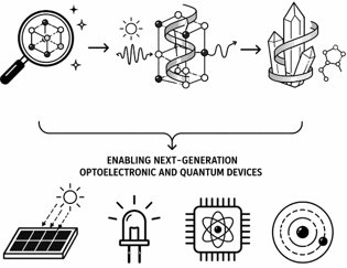
ii. Hybrid semiconducting crystal discovery – Understanding the light–matter interaction of hybrid crystals and designing new hybrid (predominantly chiral) crystals with tailored physico-chemical properties, enabling their translation into next-generation optoelectronic and (on-chip) quantum information devices.
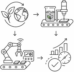
iii. Sustainable and automated processing/recycling – Developing environmentally friendly, scalable, wet and dry fabrication and recycling approaches, integrated with automation to improve reproducibility, efficiency, and throughput.
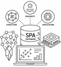
iv. Data-driven research – Constructing a comprehensive and predictive Structure–Property–Application (SPA) database of semiconducting metal halide hybrids to guide material design and device optimisation.
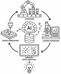
v. Automated discovery and knowledge extraction – Implementing automated workflows for materials synthesis and characterisation, device fabrication, and data analysis to accelerate discovery cycles and enable rapid insight generation.
Through this integrated approach, we aim to bridge fundamental science and technological innovation, advancing both green energy solutions and quantum optoelectronic technologies toward a more sustainable future.